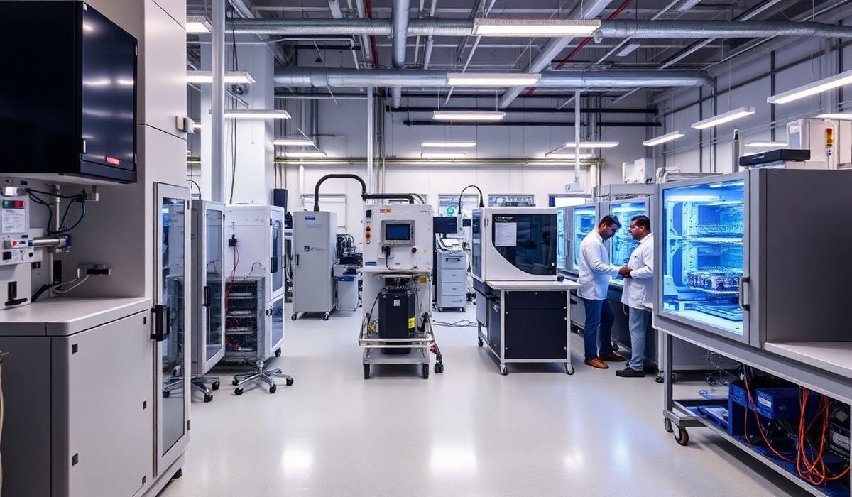
GlobalFoundries has announced the establishment of a groundbreaking Advanced Packaging and Photonics Center in Malta, New York. This is the first facility of its kind in the U.S., aimed at offering advanced packaging and testing capabilities to support domestic semiconductor manufacturing. The center’s focus includes applications in AI, automotive, aerospace, defense, and other critical industries, contributing to the country’s growing chip independence and technological leadership.
Vero’s thoughts on the news:
This initiative marks a significant step forward in bolstering the U.S. semiconductor ecosystem. Advanced packaging technologies are crucial not only for improving chip performance but also for integrating diverse functionalities into compact designs, which is essential for AI-driven applications and next-gen electronics. Establishing such a facility in New York not only supports technological innovation but also addresses vulnerabilities in the global chip supply chain. This is an exciting development that highlights the increasing intersection of hardware innovation with software-driven solutions, promising more efficient and scalable tools for developers and engineers alike.
Source: GlobalFoundries Announces New York Advanced Packaging and Photonics Center – GlobalFoundries
Hash: 90d049f3e5de43fceb1a0af49b20614fc171a094c110a5b070b8247f94494557